For some, it was a dark and dreary day. For others who languished in the geek lust of gigabytes, it was a joyous time filled with madness only Dr. Frankenstein could dream of.
Just when the iPad 2 thought it would be sold into a good home, its dreams of years of playful and continued use came to a swift and abrupt end at the hands of the devious and ravenous villains at iFixIt.com.
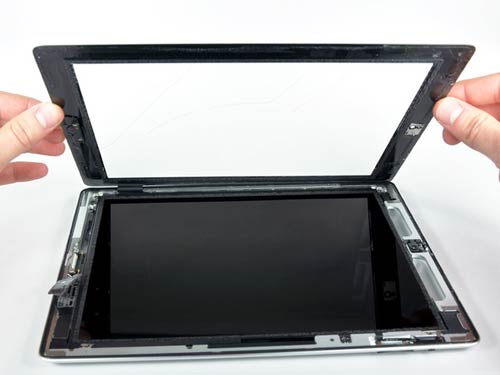
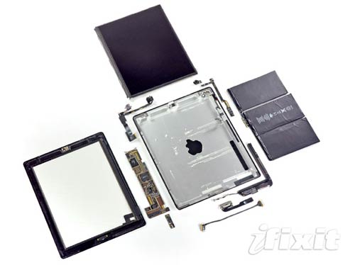
Plucked from the retail shelves of its maker, the Apple device soon was torn asunder to satiate the nerdy appetite of techies across the country. “What’s in it?”, they asked. “We’ll show you”, replied iFixIt.
The A5 processor has manufacture dates of late January and mid-February 2011. Production was clearly ramping up through the last minute. It looks like the A5 processor is the APL0498, replacing the A4/APL0398 seen in the iPad 1 and iPhones.
Ripped from its metallic insides was the central processing unit, the A5 dual-core processor.
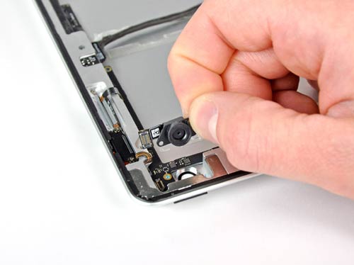
As screwdrivers took to the bearings that held the device together, iPad 2 knew it was soon to be scattered into pieces, a RAM chip here, a rear-facing camera there. No more was the tightly held together sum of its parts, iPad 2 was now rendered useless and separated.
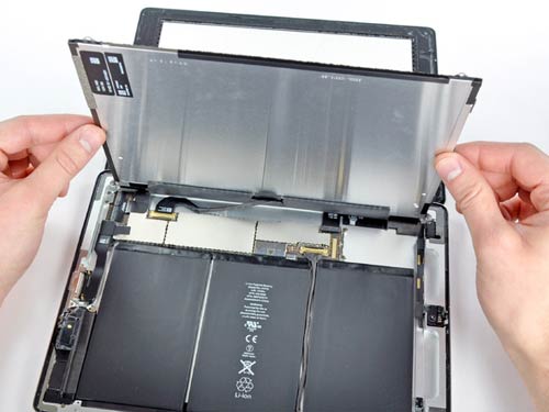
Lifting off the LCD exposes the iPad 2’s battery; A 3.8V, 25 Watt-hour unit. That’s just a hair more than the original iPad’s 24.8 Watt-hours, so any improved battery performance can be attributed to software and other hardware improvements.
The Wi-Fi board; powered by another Broadcom chip, a BCM43291HKUBC. Broadcom has made this Wi-Fi/Bluetooth/FM tuner combo chip a ubiquitous part for smartphones – lots of design wins.
But hey, that’s life. Sometimes you get the short end of the stick. And now that the gory part is over, we can finally see what’s inside Apple latest generation of the iPad tablet. Read about the complete teardown with great pictures of each step during the process.
Comment on this story | Comments Off on The Great iPad 2 Teardown of 2011